
研究活動の検索
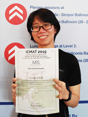
研究概要(研究室ガイド)やプレスリリース・受賞・イベント情報など、マテリアルサイエンスの研究室により公開された情報の中から、興味のある情報をタグや検索機能を使って探すことができます。学生のCHIEWさんが10th International Conference on Materials for Advanced Technologies (ICMAT)において最優秀ポスター賞を受賞
学生のCHIEW, Yi Lingさん (博士後期課程2年、応用物理学領域、大島研究室)が, シンガポールで開催された国際会議 10th International Conference on Materials for Advanced Technologies (ICMAT)(参加者約3,000人)において最優秀ポスター賞を受賞しました。
本成果は小矢野研究室(環境・エネルギー領域)との共同研究によるものです。
■受賞年月日
令和元年6月28日
■論文タイトル
Unravelling Planar Distribution of Intercalated Fe Atoms in TiS2 Layered Structure Using Transmission Electron Diffraction
■著者
Y. CHIEW, S. ABE, M. MIYATA, M. KOYANO, Y. OSHIMA
■論文概要
The discovery of new functions by intercalating guest atoms into host layered materials have attracted attention due to the wide possibilities of applications achievable. These intercalated 2-dimensional materials are known to form complex superlattices, which are difficult to analyze. For example, the material in this study, FexTiS2, has been reported to form 2a×2a or √3a×√3a superlattices for x = 1/4 or 1/3, respectively (a is the lattice constant of the TiS2 layer) where the Fe atoms occupy octahedral sites. However, in our study, a new, larger superlattice is proposed for FexTiS2 (grown with nominal content x = 0.33), based on the transmission electron diffraction (TED) pattern. TED is a powerful method that can be used to clarify two-dimensional atomic structures such as the Si (111) 7×7 reconstruction. Using the Patterson map constructed from TED pattern, the superlattice is observed to have P3 symmetry with unit lengths of √43 a× √43 a, rotated at an angle of 7.5888°. Further analysis of the TED pattern and its Patterson map also allowed the determination of the planar distribution of Fe atoms. Nine Fe atoms are found to be present in the unit cell and the Fe atoms occupy not only octahedral sites, as reported previously, but in tetrahedral sites as well.
■受賞にあたっての一言
It is a great honor to receive this award from the conference. I am extremely grateful to Prof. Yoshifumi Oshima, Prof. Mikio Koyano and Assistant Prof. Masanobu Miyata for the constant guidance. I would also like to thank the staff of Nanotechnology Platform in JAIST for their support with my sample preparation and characterization. And last by not least, I would like to thank all my lab members and friends for always being there for me.
令和元年7月3日
出典:JAIST 受賞https://txj.mg-nb.com/whatsnew/award/2019/07/03-1.html【募集終了】平成30年度 ナノテクノロジープラットフォーム公開講座「材料の構造解析のための透過型電子顕微鏡(TEM)の基礎と実習」
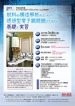
本学ナノマテリアルテクノロジーセンター主催で透過型電子顕微鏡(TEM)の技術の基礎を学び、実習を行うことのできる公開講座を開催いたします。
ただいま受講者を募集しております。皆様のご参加をお待ちしております。
| 日 時 | 平成31年3月8日(金)10:00~17:00 |
| 場 所 | 北陸先端科学技術大学院大学 ナノマテリアルテクノロジーセンター 2F会議室(石川県能美市旭台1-1) URL:https://txj.mg-nb.com/top/campusmap/ |
| テーマ | 材料の構造解析のための透過型電子顕微鏡(TEM)の基礎と実習 |
| 講 師 | マテリアルサイエンス系 応用物理学領域 教授 大島 義文 ナノマテリアルテクノロジーセンター 技術専門員 東嶺 孝一 |
| 内 容 | 透過型電子顕微鏡は、金属材料、半導体デバイス、セラミックなどの欠陥や界面といった局所的な構造や組成を知るうえで欠かせない装置です。金属材料、半導体デバイス、セラミックの特性が欠陥や界面で決まることが多いことを考えると、この装置をよく知っておく必要があります。 本講座では、透過型電子顕微鏡の原理、正しい観察手法や正しいデータ解析方法などをわかりやすく解説します。デバイスや材料の研究開発に従事している多くの方に特にお勧めできる講座です。 |
| 定 員 | 5名(先着順) |
| 参加対象者 | 企業・他大学・高専等の研究者・技術者 |
| 受講料 | 6,200 円(税込) |
| 申込方法 | 受講希望の方は、 ①氏名(ふりがな) ②勤務先等・職名 ③受講の目的 ④本講座に期待すること ⑤書類送付先 ⑥電話番号 ⑦メールアドレス を明記の上、E-mail (宛先 nano-net@jaist.ac.jp)またはFAX(ポスター2ページ目参照)でお申し込みください。 |
| 申込締切 | 平成31年2月18日(月)まで【定員に達しましたので募集を締め切りました】 |
| 問合わせ先 ・申込み先 |
北陸先端科学技術大学院大学 ナノマテリアルテクノロジーセンター事務局 〒923-1292 石川県能美市旭台1-1 TEL:0761-51-1449 FAX:0761-51-1455 E-mail:nano-net@jaist.ac.jp |
ポスターはこちらからご覧ください。ダウンロードできます。